


CVD-WS2多层薄膜 1cm*1cm
| 货号 | 规格 | 数量 | 价格 |
|---|---|---|---|
| Q-0049846 | 100mg |
1
|
询价 |
| Q-0049846 | 250mg |
1
|
询价 |
| Q-0049846 | 500mg |
1
|
询价 |
| Q-0049846 | 1g |
1
|
询价 |
| Q-0049846 | 5g |
1
|
询价 |
 17778955912
 1521565887
 1521565887@qq.com
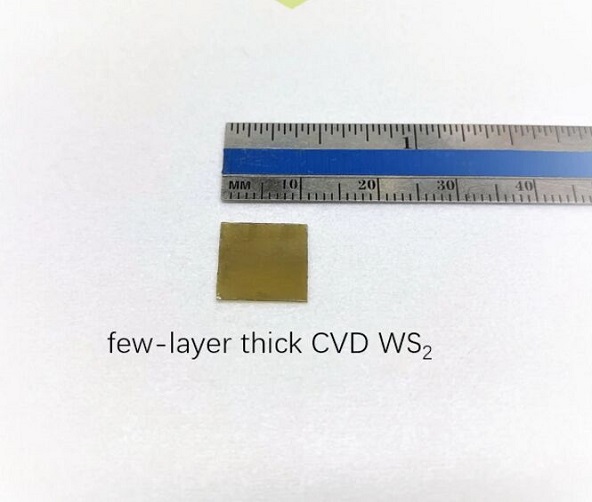
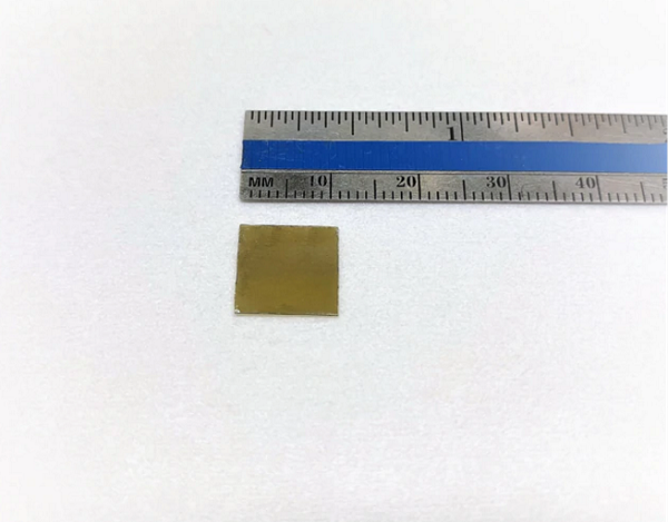
样品照片:
Raman:
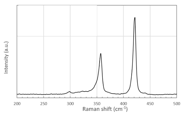
This product contains full area coverage WS2 few-layers that measure ~5 layers in thickness. Sheets are grown through chemical vapor deposition technique onto c-cut double side polished sapphire substrates, but layers can be transferred onto other substrates by polymer assisted transfer technique on demand (please select from the drop down menu). The sample measures 1cm2 in size and the entire sample surface contains few-layer thick WS2 sheet. Grown few-layers are high-crystalline as evidenced by HR-TEM, Raman, EDS, and XRD measurements. Please see the datasets in the product images.
Growth method: Our company synthesizes these few layers using chemical vapor deposition (CVD) using highest purity (6N) gases and precursors in semiconductor grade facilities to produce crystalline and large domain size samples (1-50um). Other sources typically use MOCVD or sputtering process wherein defects are very large, domain sizes are small (10nm-500nm), and products are non-layered. Our samples are always highly crystallized, high purity, and perfectly layered.
Sample Properties
| Sample size | 1cm x 1cm square shaped |
| Substrate type | (0001) c-cut sapphire |
| Coverage | Full coverage few-layer thick WS2 |
| Electrical properties | Indirect gap semiconductor |
| Crystal structure | Hexagonal Phase |
| Unit cell parameters | a = b = 0.312 nm, c = 1.230 nm, α = β = 90, γ = 120° |
| Production method | Chemical Vapor Deposition (CVD) |
| Characterization methods | Raman, photoluminescence, TEM, EDS |
| 参数信息 | |
|---|---|
| 外观状态: | 固体或粉末 |
| 质量指标: | 95%+ |
| 溶解条件: | 有机溶剂/水 |
| CAS号: | N/A |
| 分子量: | N/A |
| 储存条件: | -20℃避光保存 |
| 储存时间: | 1年 |
| 运输条件: | 室温2周 |
| 生产厂家: | 西安齐岳生物科技有限公司 |
-
二硫化钼(MoS2)是一种典型的层状过渡金属二硫属化物(TMDC),其单层结构由一个钼原子夹在两个硫原子之间构成S–Mo–S三明治式结构。层与层之间通过范德华力结合,易于剥离形成单层或少层二维结构。单层MoS₂具有直接带隙(约1.8 eV),而体相MoS2为间接带隙(约1.2 eV),这一带隙转变使其在电子与光电子领域具有独特优势。
-
二硫化钨(WS₂)是另一种重要的过渡金属二硫化物(TMDCs),其晶体结构与MoS₂类似,属于六方晶系,单层结构为S–W–S三明治式。单层WS₂具有约2.0 eV的直接带隙,光吸收性能优于MoS₂,并具有更强的光致发光能力。因其优异的光电性能与较强的抗环境氧化能力,WS₂被广泛研究用于光电器件、催化、电池及气体传感器等领域。
-
CVD-MoSe2多层薄膜 1cm*1cm
-
CVD-PdS2薄膜
 官方微信
官方微信 官方微博
官方微博